ASML’s longer mask targets 40% speed gain
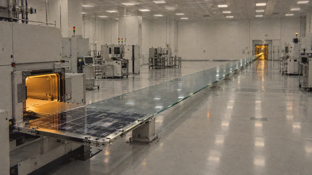
A longer mask asks an entire factory to change shape.
Image composition · tobriefToday’s standard photomask is too short for a High-NA scanner to expose the conventional full chip field in a single pass. ASML and TSMC propose a longer mask to recover that field, but their joint announcement sets a development roadmap rather than reporting a working production system.
Better detail, but a smaller canvas
A photomask is the master template for each layer of a chip. A lithography scanner projects its pattern onto a light-sensitive coating on a silicon wafer, allowing later manufacturing steps to turn the image into circuitry.
High-NA improves the scanner’s ability to distinguish tiny features. “NA” means numerical aperture, a measure of the range of light angles the optics can accept. Think of a microscope objective gathering light from more directions: those extra angles help it separate details that would otherwise blur together. Imec has demonstrated finer patterning with High-NA.
That improvement creates a geometrical trade-off. Conventional EUV optics shrink the mask pattern equally from side to side and top to bottom. High-NA’s mirror arrangement shrinks it more strongly along the scanner’s direction of travel. With the current mask, the image therefore covers only half the conventional field along that axis.
A chip layer extending beyond that shorter field must be divided between neighbouring exposures. The scanner then aligns the images at an internal seam, a process called “in-die stitching” that researchers are testing experimentally.
The proposed rectangular mask adds pattern space along the squeezed direction. After the optics reduce that longer image, it can fill the conventional field again. For a qualifying layer, it could replace two stitched exposures with one. It would not enlarge the chip or increase the number of chips on each wafer by itself.
Where the speed gain could come from
ASML has projected an approximately 40% throughput gain when the larger mask replaces a stitched process. The logic is straightforward: eliminating the repeat exposure lets the scanner begin the next wafer sooner.
That figure remains ASML’s forecast, not an independently measured production result. It applies to layers that would otherwise need stitching; designs already fitting inside the shorter field have little to gain from the mask change. Nor does a quicker exposure automatically improve manufacturing yield, the share of chips that work.
The scanner technology is further along than the new mask. Imec has taken experimental patterns through metal deposition and electrical checks, showing that selected structures survived fabrication beyond the initial printed image. Printing tests whether the scanner can resolve a pattern; the later work tests whether that pattern can become a functioning electrical structure. The large-mask announcement reports no comparable end-to-end demonstration.
The longer plate changes an industry
The mask may look like a larger piece of glass, but using it requires an ecosystem conversion. Suppliers need compatible tools for making, inspecting, protecting, transporting and loading it. ASML, chipmakers and equipment suppliers must agree on a shared format and prove that every hand-off preserves the cleanliness and precision EUV requires.
The roadmap aims for pilot-line readiness by 2031, paving the way for systems to enter production from 2033. Those are development targets, not evidence that the pilot has been built or the production chain qualified.
Chipmakers do not plan to wait for the new format. Samsung has outlined a 2028 High-NA plan for advanced memory, while TSMC’s roadmap places High-NA manufacturing from 2030. Existing masks and stitching will carry the early transition.
The longer format is designed to recover High-NA’s full field and remove a stitch for qualifying layers. Turning that into a real productivity gain now depends on ASML, chipmakers and equipment suppliers qualifying the same physical format across an entire factory chain.
Details about this article
- Model:
- gpt-5.6-sol
- Generated:
- 9/9/2026, 9:37:18 AM
- Pipeline run:
- eu_pipeline_20260909_005005
- Watermark:
- SynthID (Google's invisible watermark)
- Human review:
- None before publication