Sub-5nm transistors reach four-inch wafers
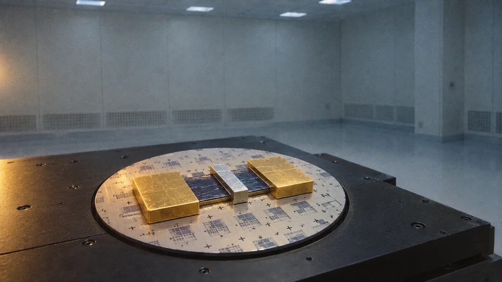
An atom-thin switch moves from laboratory scale toward the production line.
Image composition · tobriefEvery processor is built from transistors, tiny electrical switches, and chips have long improved by making those switches smaller. A team led by Carnegie Mellon University has now built transistors from a single atomic layer of molybdenum disulfide (MoS₂), with channels shorter than 5 nanometres, and implemented the process on a four-inch wafer (Nature Communications). The peer-reviewed result pairs extreme miniaturisation with the patterning method chip factories use.
The work also involved the University of Florida, MIT, Texas A&M, the University of Southern California and Spain's Universidad Politécnica de Madrid (Semiconductor Engineering).
Keeping the gate in charge
Current in a transistor flows from one terminal, the source, to another, the drain, through a strip of material called the channel. A third electrode, the gate, controls that flow by raising or lowering an energy barrier. Picture it as a hill that electrons must climb: raise the hill and the switch is off, lower it and current flows.
Shrink the channel far enough and the source and drain sit so close together that their own electric fields start flattening the hill. The gate loses sole control, and current leaks through when the switch should be off, like a tap that never fully closes.
The team's approach relies on thinness. In a channel only one layer of atoms thick, the gate's electric field acts on the entire channel at once, so no part of the material sits out of its reach (Nature Communications).
How sharp is the switch?
Engineers judge a switch's sharpness with a figure called subthreshold swing. It measures how much extra gate voltage it takes to multiply the current tenfold as the device turns on. A smaller number means a sharper switch, and a sharper switch can, in principle, run at lower voltage (Nature Communications). This study did not demonstrate a low-voltage circuit.
For the devices they tested, the authors report a swing of 88 millivolts per decade, and an "on" current more than a million times the "off" current (Nature Communications). The summary doesn't say whether 88 is the best, typical or median value. The on/off ratio carries the real message. A device this small that only conducted would just be a wire, and these still switch.
The paper's title describes performance "beyond the silicon limit." That phrase doesn't mean the devices beat the thermal floor of about 60 millivolts per decade that bounds conventional transistors at room temperature (review). At 88, they sit above it. The comparison with silicon is the authors' own framing.
From record devices to a wafer
Earlier experiments had already pushed MoS₂ transistors to remarkable dimensions, including channels under 10 nm (Nano Letters) and a gate electrode about one nanometre long (Science). The new work adds a production-style method to that miniaturisation. The team used photolithography, which draws circuit patterns by shining light through a stencil-like mask onto a light-sensitive coating. It is the same basic technique chip factories rely on.
The authors describe the process as compatible with CMOS fabrication, the manufacturing flow behind nearly all digital chips. In their account, the steps are designed to fit alongside conventional silicon processing. They ran it on a wafer about 100 mm across (Nature Communications), a detail Semiconductor Engineering repeats in its summary of the paper (Semiconductor Engineering).
This is a wafer-scale fabrication demonstration. Production readiness would require yield and variation data, which the published summary does not give, and the accessible record does not establish that the transistors were connected into circuits. A separate study on larger 300-mm wafers, using longer MoS₂ and WS₂ devices, shows what the next stage involves. It reached roughly 95–99% yield, yet still found high contact resistance, the electrical loss where metal wiring meets the atom-thin layer, along with variation from one wafer to the next (300-mm study).
This peer-reviewed work shows that sub-5-nanometre MoS₂ channels and wafer-scale lithography can coexist in one process (Nature Communications). Yield and device-to-device variation will determine whether that process can become a manufacturing platform.
Details about this article
- Model:
- claude-opus-5-5
- Generated:
- 9/23/2026, 6:52:34 AM
- Pipeline run:
- eu_pipeline_20260923_005006
- Watermark:
- SynthID (Google's invisible watermark)
- Human review:
- None before publication